PCBs are used in pretty much every electronic device, and even though these components may seem simple and easy to manufacture, in reality, there are a lot of things that need to be planned for and paid attention to during the construction process. As you already know, there are many different types of designs and layering of the printed circuit boards, and here we are going to talk about some electrical engineering basics and things related to these units.
Keep on reading if you want to learn some of the things that you should know about PCB assembly, what is the way that a manufacturer can prepare to finish this task properly, and which steps are taken to construct the boards.
1. Things required for the assembly process
Before starting the construction process, a plan needs to be made on where things are going to be placed and how to make sure that any potential errors or issues are avoided or minimized.
The first thing that needs to be considered is the components and their layout. Note that some components are going to require heat sinks, and they should be properly spaced so there is no overheating or risk of melting.
Then the hole and vias spacing needs to be considered and the solder pad should never get in contact with the hole. Finally, the thickness, the copper pad, as well as the width of the trace needs to be planned, and the manufacturing facility needs to create exact solutions for every design of the printed circuit board so there are no problems during the production process, the tests, or the inspection.
Know that even though this seems complex, once the plan is created for a certain type of PCB, the same outline can be followed when that model is constructed. In most facilities, depending on what they manufacture, there are separate plans and outlines for all the models that are manufactured there, and this process does not have to be repeated for every single batch of PCB.
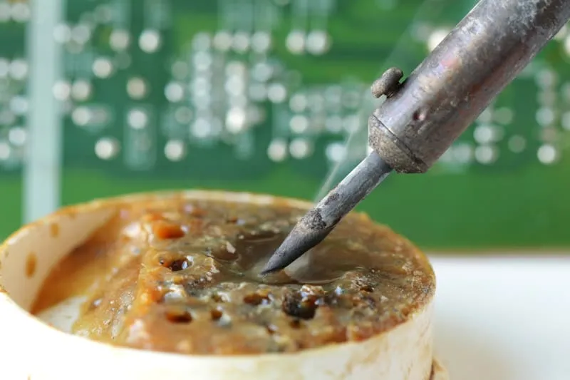
2. First PCBA step – soldering paste
When it comes to the exact construction process, there are several things that are going to be the same for every type of board, no matter how simple or complex it is. On the same note, things may differ depending on the design, and sometimes this process may be really simple or extremely complicated.
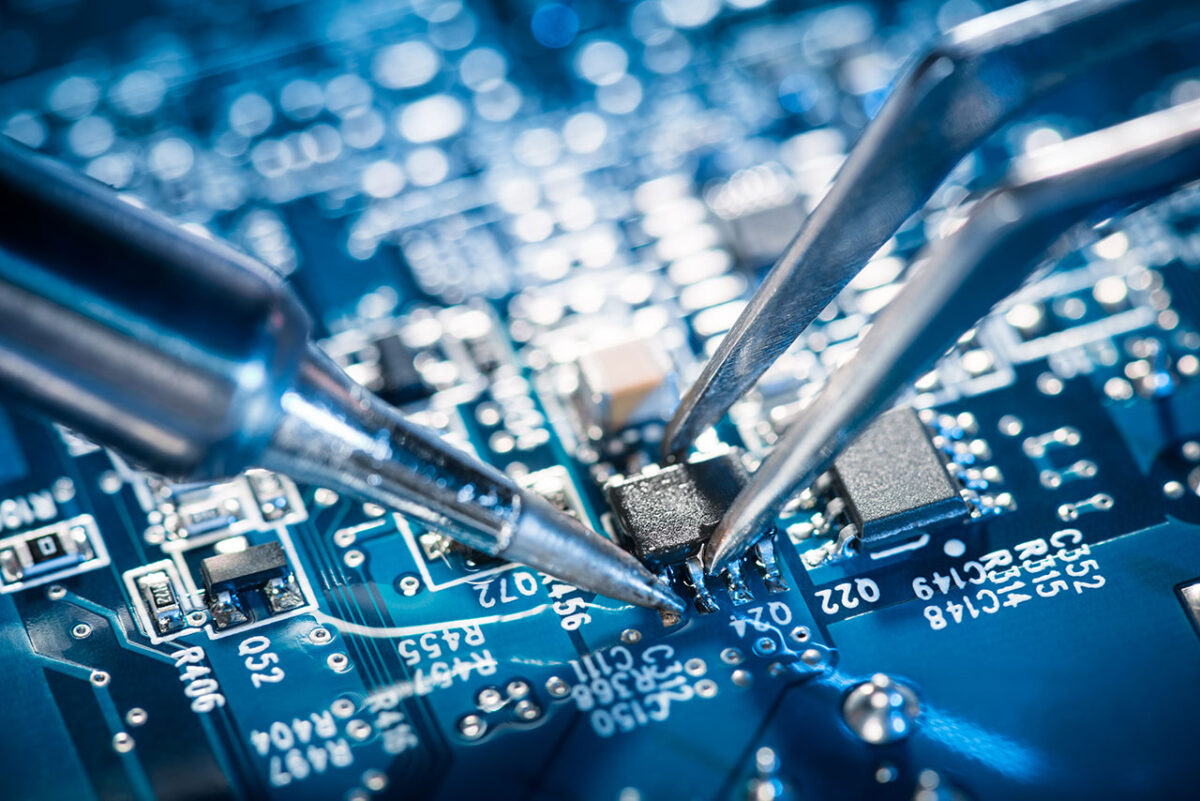
The first thing that is done is applying the solder paste, and for this, a stencil is most commonly used. Stencils help keep everything under control, and there won’t be any waste or errors while applying them. Note that the right amount of paste needs to be used so that there won’t be any lack or, once again, waste.
3. Second PCBA step – installing components

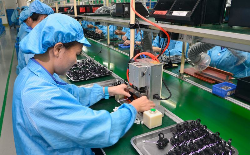
In most manufacturing facilities, the next step is putting the components using automated systems or robots. The reason for this is so that it saves a lot of time, instead of installing them manually, and the risk of anything getting damaged is minimized. All of the components that are needed will be properly placed and spaced out, so there won’t be any difficulties in the next parts of the construction.
The most advanced facilities nowadays will make sure that they offer their customers reliable turnaround times and exceptional value for the boards that are manufactured.
Find more information on pcb assembly at https://vinatronic.com/
4. Third PCBA step – reflow soldering and baking
Then the components are set, and after that reflow soldering is done. This is finished by putting everything on a conveyer belt and the board along with the components goes through an oven that is usually set to 250 degrees Celsius.
When the board leaves the oven, then it is placed in coolers that solidify all the components on the PCB and with that, the main assembly process is done. Note that in some cases, depending on the complexity of the design, some of the steps may be repeated for every layer of the board.
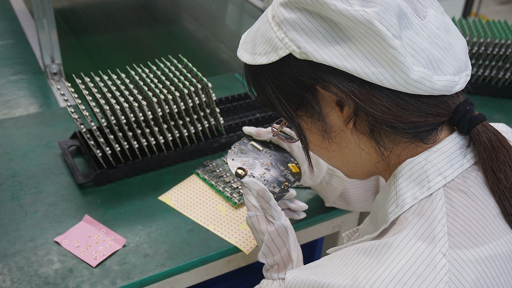
5. Fourth PCBA step – inspection
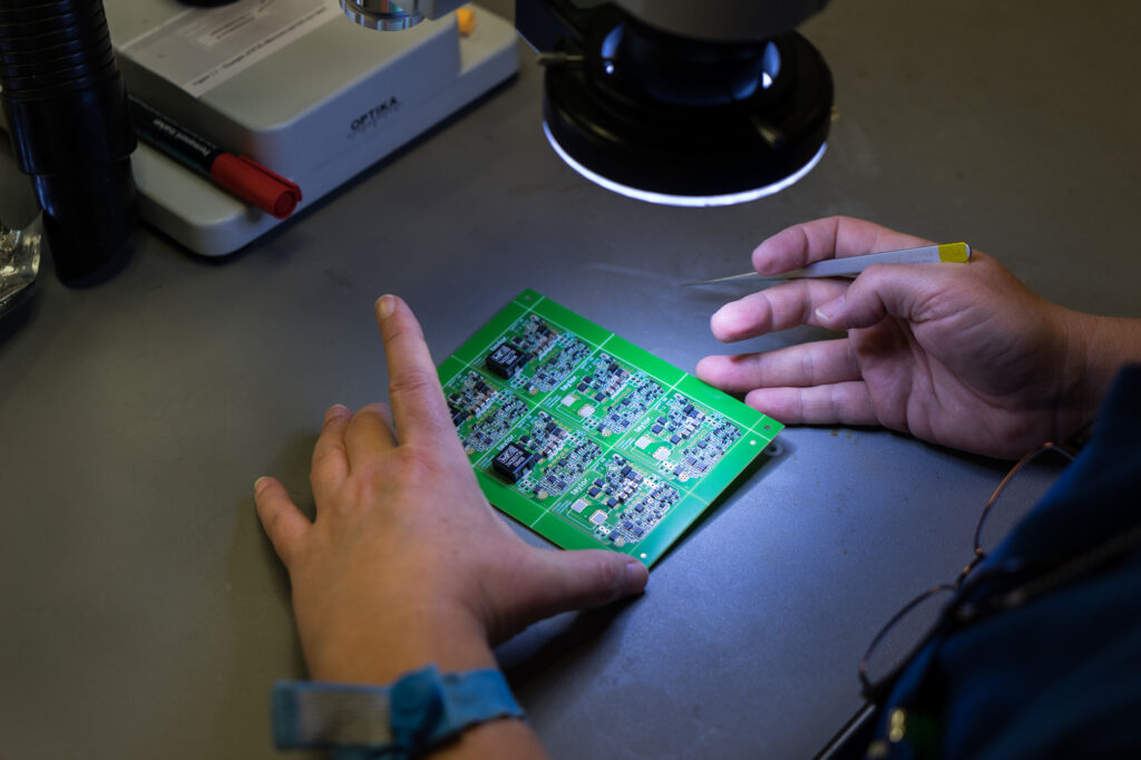
Once the assembly is done, the next part is the inspection. Even though everything is done automatically, during the movement of the boards there might be some movement of the components, so every board needs to be checked to make sure that things are in the right place and that the unit will function properly after it is installed in the device.
There are three main types of inspection and they include manual inspection where the workers check to see if everything is done as it should be, optical one, where this is done with the help of machines that check if everything seems right, and finally, x-ray inspection.
6. Fifth PCBA step – testing
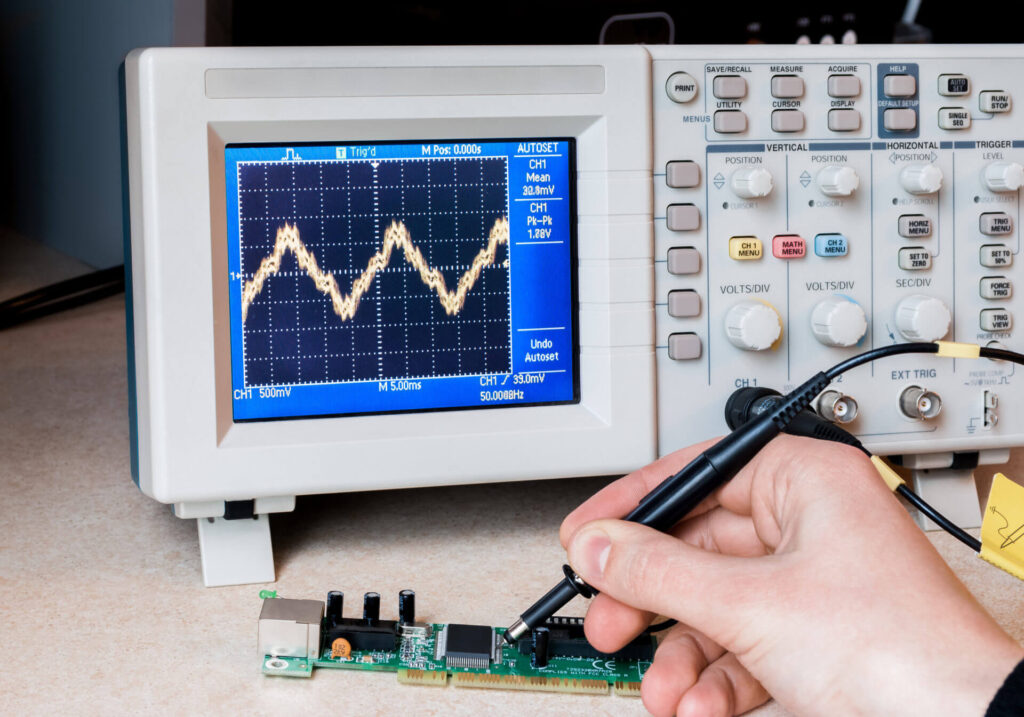
Once the inspections are done, and the boards look like they are the way that they are supposed to be, a functional test is done, and here, the employees in the manufacturing facility will make sure that the PCB functions in the way that it is supposed to. Note that in case any of the boards don’t perform in the way that they need, then they are either discarded or their components get removed and they get reused for some other PCB.
Finally, all of the boards that are working properly and that have been cleared for release, are going to get cleaned, finished, packed, and then shipped to other facilities.
Know that the assembly process is pretty complex, and even though most of the things are done using equipment and robotic devices, still components, placements, and tests need to be done by human workers. With the advancement of technology, this process is made much faster and easier, and it is expected in the future things to be even more advanced. It is crucial to collaborate with a manufacturing facility that does every step of the process correctly and that conducts all the needed tests and inspections. If you have any questions about the process or any specific steps, you can always reach out to the professionals to make things more understandable for you.